
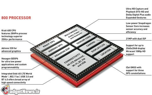
با معرفی پروسسور اسنپ دراگون ۸۰۱، شرکت کوالکام سردرگمی هایی را در بخش پردازنده ها ایجاد نمود. در ابتدا بسیاری از ما فکر میکردیم که کوالکام تنها این پردازنده را بدون هیچگونه تغییر آنچنانی نسبت به اسنپ دراگون ۸۰۰ معرفی کرده است. براساس اطلاعات کسب شده پردازنده اسنپ دراگون ۸۰۰ در سه نسخه مختلف ۸۹۷۴VV, 8974AB, 8974AA در بازار وجود دارد، همانند اسنپ دراگون ۸۰۱ که آن هم در نسخه های مختلف در دسترس قرار داد.
وبسایت AnandTech که همیشه بخوبی مسائل مربوط به پردازنده ها را پیگیری میکند، جدولی را منتشر کرده که براساس آن براحتی می توان به تفاوت بین نسخه های مختلف دو تراشه اسنپ دراگون ۸۰۰ و اسنپ دراگون ۸۰۱ پی برد.
همانطور که مشاهده می کنید، تفاوت عمده بین این تراشه ها در کلاک اسپید CPU و GPU آنها می باشد. علاوه بر آن پردازنده های اسنپ دراگون ۸۰۱ از eMMC 5.0 و DSDA/ Dual SIM, Dual Active پشتیبانی می کنند، این بدان معنی است که با استفاده از پردازنده های جدید می توان تا دو سیم کارت برروی اسمارت فون داشت و هر دو را فعال نگه داشت.
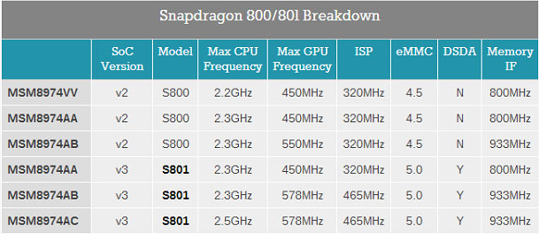
همچنین نسخه های AB/AC پروسسور اسنپ دراگون ۸۰۱ دارای رابط سریعتر LPDDR3 می باشند که این ویژگی باعث می شود تا اپلیکشن های پیچیده ای چون بازی های ۳D و پردازش های مربوط به تصویر و دوربین راحتتر و بهتر انجام گیرد.
یکی از نکات جالب در مورد نسخه های مختلف این پردازنده های این است که قوی ترین نسخه اسنپ دراگون ۸۰۰ تاحدودی عملکرد بهتری نسبت به ضعیف ترین عضو اسنپ دراگون ۸۰۱ دارد، پس استفاده از نام اسنپ دراگون ۸۰۱ در محصولات مختلف به معنی بهتر بودن این پردازنده نسبت به اسنپ دراگون ۸۰۰ نیست، مخصوصا اگر این دستگاه قابلیت پشتیبانی از تنها یک سیم کارت را داشته باشد.
منبع : anandtech
The Difference Between Snapdragon 800 and 801: Clearing up Confusion
A couple of weeks ago at MWC, Qualcomm announced its Snapdragon 801 which was positioned as a speed bump for the next wave of flagship smartphones. Qualcomm touted a 2.5GHz CPU frequency (up from 2.3GHz with Snapdragon 800), as well as increased GPU, ISP and memory interface speeds. Samsung announced immediate support for the new Snapdragon 801 with the Galaxy S 5, as did Sony with the Xperia Z2. Unfortunately this is where confusion set in. The Galaxy S 5 was advertised as a Snapdragon 801 with a 2.5GHz CPU clock, while the Xperia Z2 claimed the same Snapdragon 801 branding but with a 2.3GHz CPU clock – the same frequency as a Snapdragon 800. If it's not CPU frequency that separates a Snapdragon 800 from an 801, what does? The answer, as it turns out, is a little more complex. The table below should help explain it all:
The Snapdragon 800 brand applies to an internal Qualcomm model number of MSM8974. The MSM8974 has four Krait 400 CPU cores, an Adreno 330 GPU, dual-ISP, 64-bit wide memory interface and a 9×25 Cat 4 LTE modem. It turns out there are two different silicon revisions of this SoC: version 2 and 3. The Snapdragon 800 v2 silicon was made available in three different flavors: VV, AA and AB. The difference between all three MSM8974 v2 variants was CPU and GPU frequency. This isn't an unusual practice at all as there's bound to be a distribution of operating frequencies for any design. Better bins end up as higher clocked parts, while others get tested and pass at lower frequencies. OEMs can pay more for the faster bins if they want.
In the case of v2 silicon, you could end up with silicon that ran its CPU cores up to 2.2GHz or 2.3GHz. Only the AB variant saw its max GPU frequency climb to 550MHz. The rest of the specs remain identical between all v2 silicon (-AB does get access to faster DRAM). Note that I'm using the marketing frequencies here for CPUs and not the actual frequencies. For whatever reason the OEMs choose to round up to the nearest 100MHz when quoting CPU speeds (2.2GHz is actually 2.15GHz, 2.3GHz is actually 2.26GHz and 2.5GHz is actually 2.45GHz). That's a battle for another day.
Over time it's possible to squeeze more out of a given process and that's exactly what Qualcomm did with MSM8974 v3. This newer silicon revision used improvements on the process side (process push of 28nm HPm) to push frequencies even higher. The options are now 2.3GHz and 2.5GHz on the CPU side. Just like with v2, v3 silicon offers three different variants. Unlike the situation with v2, v3 sees increases in CPU, GPU and ISP operating frequencies depending on which bin an OEM orders. Note that the increases in ISP frequency are substantial. If my math is correct, the Snapdragon 801 should be able to push almost as many pixels through its ISP as the forthcoming 805.
The other major difference is that v3 silicon enables support for eMMC 5.0.
In short, there are two different versions of MSM8974 silicon. Version 3 adds eMMC 5.0 support and hardware dual-sim, dual-active (DS-DA). All variants of v3 silicon can carry the Snapdragon 801 branding, while all v2 variants are Snapdragon 800s.
Putting it in Perspective
What does all of this mean? Let's first talk about the non-frequency related benefits of MSM8974 v3. eMMC 5.0 adds some new features as well as increases the maximum interface speed from 200MB/s in eMMC 4.5 to 400MB/s. As high end smartphones and tablets start using faster internal storage, having eMMC 5.0 support will be necessary to enable faster transfer speeds. SanDisk's recently announced iNAND Extreme update promises 300MB/s sequential read performance for 32GB+ devices. On a smartphone equipped with USB 3 that means you could feasibly copy large movies or files off of your smartphone at up to 300MB/s. Without eMMC 5.0 support you'd be limited to somewhere south of 200MB/s.
DSDA support matters to specific regions, and for those areas the benefit is obvious.
Supporting faster LPDDR3 means more available memory bandwidth for all of the big consumers on the SoC. I'd expect improvements in high end 3D gaming performance, and potentially certain camera/imaging workloads. Remember that all parts of the SoC have to share that tiny interface to main memory, so more memory bandwidth definitely doesn't hurt.
On the frequency side, the gains are pretty easy to understand. The higher peak CPU speed will translate into faster web page and application loads. Higher GPU frequency will allow for smoother frame rates in 3D games, and the faster ISP frequency can enable quicker processing of camera sensor output. You can also look at the benefits of these things from the perspective of lowering power consumption. Tasks can now complete in less time, allowing these individual IP blocks to quickly move down to lower power states and increase battery life.